Graphite along with other materials such as pyrolitic boron nitride (PBN) and Silicon Carbide (SiC) have been used in processing for many years where their combination of purity and resistance to chemicals and thermal shock mean they are ideally suited to the unique requirements of the semiconductor manufacturing process. Despite their effectiveness, further innovation in ceramic-based materials is being driven by the need to reduce cycle times and reject rates in this competitive sector.
While ceramic materials are rarely used in the ‘slicing’ process that creates individual ‘wafers’ from the monocrystal silicon ingots, they come into their own in the subsequent wafer processing steps including ion implantation, deposition and etch processes, which introduce successive conducting and insulating layers into the wafer before it is broken down into individual chips.
The need for precision in the process has increased greatly as the size of connectors has dramatically reduced, from typically 30 nanometres (nm) to around 10nm. This issue is exacerbated by the desire to process larger individual wafers to increase overall productivity. The move towards the processing of 450mm wafers places greater demands on both materials and components.
Being thin and fragile, the wafers need careful physical handling, while the need for cleanliness is vital to prevent the introduction of contaminating particles into the wafer
In most production facilities the wafers are moved between individual processing stations by a robot. Being thin and fragile, the wafers need careful physical handling, while the need for cleanliness is vital to prevent the introduction of contaminating particles into the wafer.
Key to the handling process is the ‘end effector’ on the robot arm, responsible for picking up the wafer and transporting it between stations for processing. The end effector must have a good ratio of weight to stiffness and be as pure as possible to minimise the risk of contamination to the wafers during processing.
There are two main choices for specifiers for the material for the end effector: aluminium and aluminium oxide (alumina) ceramic. However, where aggressive chemicals may be present, aluminium is not a good choice as it is difficult to keep clean due to its propensity to react chemically with cleaning media, deforming the end effector and potentially introducing further contaminants to the process.
Aluminium also presents physical issues for wafer handling operations. Its higher inertia can lead to less accurate movements at higher rates of motion, and it is relatively fragile and can be deformed easily. This deformation means that when the end effector picks up the wafer, it may not be correctly positioned. The deformation may also not be noticeable to the naked eye, meaning multiple parts can be processed before the issue is spotted.
By contrast, high purity alumina can be ‘clean-fired’ to remove trace contaminants and offers reduced risk for specifiers and system designers. Boasting excellent strength and able to be cleaned with chemicals with no physical effects, alumina end effectors are very stiff at lower masses, and so reduce the inertial problems associated with aluminium products. This allows faster robotic movements with a shorter settle time to an accurate position. The issue of deformation is negated too, as an alumina end effector will not deform at all until it reaches the point at which it physically fractures.
Alumina offers benefits in other areas, not least in the physical design of the end effector. In an attempt to reduce cycle times and make the process ‘intelligent’, there is a growing demand for end effectors to be fitted with optical detectors that can scan the entire cassette and move the robot arm automatically to the correct position to pick up or deposit a wafer. Meanwhile, manufacturers are also seeking smaller, thinner end effectors with the same vacuum capacity. The extra machining required to incorporate one or both of these features, would be very difficult with aluminium but achievable with alumina due to the latter’s greater strength at lower thicknesses.
Deposition
For the deposition process, the chamber wall must be chemically inert and also physically stable at high temperatures. Here, specifiers usually face a choice between a zirconia and alumina chamber liner. While zirconia is effective, it is more expensive, and not so easy to adapt to individual requirements. Alumina, with a purity of 99.5% or higher, has very strong dielectric qualities and is easily shaped to customer requirements.
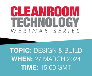
MTC Auburn deposition ring
Another recently available capability is the application of a textured coating for reduced particle generation in CVD chambers with the aim of reducing mean time between maintenance. As wafer throughput increases, film from the wafer is deposited on to the chamber walls and other internal alumina components. The texturing of these surfaces helps to prevent the film particles from flaking off and contaminating the wafer. This technology offers significant advantages over techniques such as bead-blasting, whose roughening action can cause lasting physical damage to the surface, reducing service life. The textured coating has a rounded morphology, containing the particles better than the sharper morphologies created with bead blasting.
For etch reactors, the chamber walls are also frequently treated with coatings to enhance their resistance to fluorine etch gases. Traditional technologies in this area focus on the use of plasma-coated yttria, which creates a mechanical bond with the substrate. However, recent innovations have created a yttria coating for the chamber dome and rings that is covalently (or chemically) bonded to the alumina substrate. This prevents delamination or the bond failing.
Purity and performance
Graphite is used for a variety of applications in semiconductor processing, including components for ion implanters and as metal organic chemical vapour deposition (MOCVD) susceptors. Key to the success of materials used in these applications is their purity (to avoid particle contamination and maximise wafer yield), and the extent to which this can be achieved without prohibitive cost. Graphite has dimensional integrity at very high temperatures, as well as high chemical resistance, and desirable electrical and mechanical properties.
Modern graphite purification processes are able to reduce impurities to 2–3ppm and are cost-competitive compared with the use of alternative materials
Modern graphite purification processes are able to reduce impurities to 2–3ppm and are cost-competitive compared with the use of alternative materials such as molybdenum, tungsten and tantalum. They are also typically more difficult to machine and more expensive than graphite, whose other refractory properties make it more suitable for interior components.
Chemical Vapour Deposition (CVD) silicon carbide (SiC) is a very high purity (99.9995%+) material used in semiconductor process applications where long service life, high thermal conductivity, and plasma erosion resistance are required. CVD SiC is particularly suited to applications such as wafer edge rings for rapid thermal processing, shower heads and focus rings for etch chambers, and as wafer carriers in MOCVD tools.
CVD SiC wafer carriers for MOCVD applications offer unmatched erosion resistance in the high-temperature ammonia environment present in these tools. The material purity is also an advantage compared with conventional SiC-coated graphite wafer carriers, which can contaminate the MOCVD chamber once the ammonia eats through the coating and exposes the graphite.
Modern manufacturing methods enable the production of a superior quality CVD SiC with monolithic substrates meaning there is no film interface where thermal mismatch and ultimately adhesion failure can occur.
Similarly, pyrolytic boron nitride (PBN) products are available with high purity, offering premium electrical resistivity, dielectric strength, chemical resistance and the ability to operate at temperatures in excess of 1500°C. Modern CVD PBN materials are particularly suited to crystal growth and effusion cell environments for metal evaporation. Common applications for this material include vertical gradient freeze crystal growth of gallium arsenide materials, and aluminium cathode evaporation in the production of organic light-emitting diode large displays.
Optimised surfaces
Innovations in ceramics for semiconductor applications focus on the optimisation of surfaces that can now be textured on components for ion implantation machines, which are located at key points along the beam path to collect particulates and prevent them from contaminating the wafer downstream. Meanwhile, glassy carbon impregnation increases the density of the substrates, eliminating the presence of surface particulates, improving wear and erosion resistance.
Graphite components can also be treated with a glassy carbon coating which again negates the production of surface particles, reducing sealed surface porosity and permeability while offering excellent release characteristics. These attributes are key as they help reduce cycle times because the part does not ‘out-gas’ during the pump-down cycle.
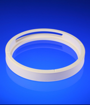
An Allentown Diamonex Phoenix pad conditioner
Other types of coating are making a difference to product performance and life too, particularly when combined with modern substrate materials. In the area of Chemical Mechanical Planarisation (CMP) products, for example, the typical choice of substrate for CMP conditioners has been stainless steel, but this is prone to corrosion during the CMP process. For this reason plastics and ceramics such as reaction bonded (RB) SiC have become an alternative option. The benefits of RBSiC are the strength and purity achievable, as RBSiC does not introduce foreign elemental materials into the production process.
The CMP conditioners’ abrading surfaces can now be executed with structural ‘edge’ features on the surface, instead of diamond abrasive, in a monolithically designed RBSiC part. The top surface then receives a pure CVD diamond coating for abrasion resistance. Therefore, unlike other diamond products, it does not contain a diamond grit that could detach from the substrates and cause defectivity on the wafer.
Abrasion is now being performed solely with the CVD diamond coated RBSiC surface, greatly minimising the presence of trace metal contaminants such as nickel and cobalt.