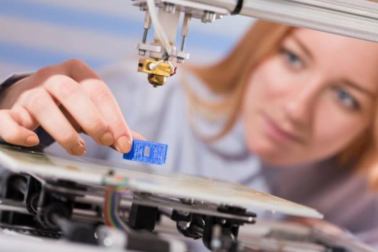
3D printing has shown great potential in laboratories for making customised labware at a low cost, based on open source hardware design and affordable materials. For example, digital recreation of devices with 3D printing has been used in the fabrication of reactionware, millifluidics, microfluidics, and continuous flow chemistry equipment, and for advanced characterisation techniques like mass spectroscopy. Indeed, fused filament fabrication (FFF)-based 3D printing has successfully produced high-quality scientific equipment affordable. In general, this approach reduces capital cost of scientific equipment by 90%-99% compared to conventionally produced equipment.
However, the applicability of 3D-printed devices to cleanrooms used for semiconductor processing is not as straightforward. Many scientists and engineers have been reluctant to use 3D-printed tools inside clean environments due to concerns around the chemical compatibility or particle generation. But that’s about to change. Two recent studies – one on chemical compatibility and the other on particle generation – demonstrate that 3D-printed objects are not notable contamination sources, and hence, are equally suitable for use in cleanrooms as the commercial equivalents.
3D-printed accessories based on individual process requirements have the potential to improve cleanroom throughput as well as reducing processing costs
Findings showed that 3D-printed plastics are potential materials for bespoke chemically resistant labware at less than 10% of the cost of such purchased tools. In addition, the results showed that case studies of 3D-printed units generate as little particles as commercial equivalents. Elemental analysis revealed that 3D-printed objects contain no other harmful metal impurities than those originating from colourants.
3D printing scientific tools
The exact chemical formulation of low-cost commercial 3D printing filaments (as well as additives such as plasticisers and colourants) is proprietary and thus chemical compatibility of printed parts was unknown. In addition, no one knew if 3D-printed products could meet the extremely strict cleanliness requirements to prevent contamination of cleanrooms.
In a multidiscipline research-orientated cleanroom and industrial R&D facilities, significant time is spent on overcoming equipment limitations; equipment is installed to serve a wide range of research interests instead of the optimum for every process. Thus, 3D-printed accessories based on individual process requirements have the potential to improve cleanroom throughput as well as reducing processing costs by, for example, reducing the consumption of chemicals needed for processing.
To exploit these opportunities, Aalto University completed two studies to provide laboratory and cleanroom staff with a materials toolkit for making their own reliable, customised, and chemically resistant labware from affordable supplies using accessible FFF-based 3D printers as alternatives for commonly used polypropylene and fluoropolymer tools.
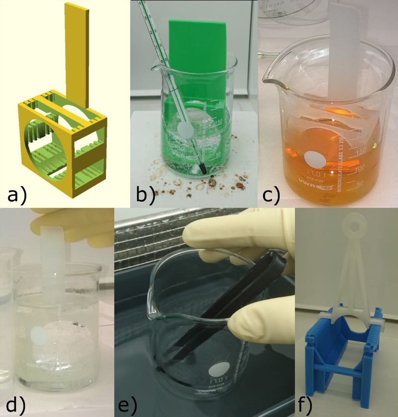
Examples of 3D-printed labware: a) 3D model of the 2-inch dipper; b) Modified dipper made of green ABS in RCA 1 solution in a borosilicate beaker; c) Clear PP dipper in Aqua regia solution; d) PP dipper immersed into Piranha,
e) Black Alloy 910 tweezers in sonicated acetone; f) a large clear PP handle for a 3 inch wafer jig
Chemical compatibility
The first study evaluated the chemical compatibility of 3D printing polymers with wet chemical treatments commonly used in the cleanroom processing of semiconductor devices.
The 3D printing materials considered include:
- Polylactic acid (PLA)
- Polyethylene terephthalate glycol (PETG)
- 2 different co-polyesters (Eastman Amphora AM3300-based nGen and Amphora 1800-based Inova-1800)
- Polypropylene (PP)
- Acrylonitrile butadiene styrene (ABS)
- Acrylonitrile styrene acrylate (ASA)
- Polyamide copolymer-Nylon 6/69 (taulman3D Alloy 910)
- Polyethylene terephthalate (PET, taulman3D t-glase)
- Polycarbonate (PC)
Each 3D-printed polymer went through a multi-phase process: Phase I is the immersion of filaments in a single chemical, while in Phase II, 3D-printed rectangular pieces of the materials that showed acceptable compatibility were immersed in the same chemicals. Based on the results of both phases, suitable 3D printable materials were selected for case studies based on their chemical tolerance and ease to print.
The simple chemicals tested in the first phase are deionized water (DI H2O), isopropyl alcohol (IPA), acetone, ethanol, hydrochloric acid (HCl, 37%), ammonia (NH3, 25%), hydrogen peroxide (H2O2, 30%), phosphoric acid (H3PO4, 85%), nitric acid (HNO3, 69%), sulfuric acid (H2SO4, 95-97%), and acetic acid (100%).
While many of the chemicals are generally used as dilute solutions, the 3D printable plastics are immersed in concentrated solutions to study the upper limit of their chemical compatibility. If a plastic is compatible with a concentrated solution, it will most likely tolerate diluted solutions of the same chemicals for extended times.
Printed samples that passed the tests were analysed with differential scanning calorimetry (DSC) to evaluate changes in the crystallinity, glass transition and melting temperatures of the polymers, which are closely linked to, amongst other factors, polymer chain structure, repeating unit type and length, molecular weight, branching, additives, etc.
The materials that withstood the simple chemical environments were then tested in more demanding chemical processes and solutions commonly used in semiconductor device fabrication.
Figure 1 summarises the results of the chemical immersion experiments and compares them to the literature. The leftmost column represents reported compatibility of the polymer with the chemical in the literature (L), while the center and the rightmost column present the results from chemical immersion tests for pure filaments (F) and 3D-printed (P) samples in this study, respectively.
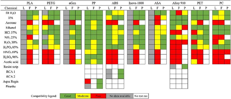
Figure 1. Map of chemical compatibility of plastics and 3D printing materials from the literature (L), as virgin filament (F) and 3D-printed (P)
Literature compatibility has been assessed by comparing different chemical compatibility charts published by polymer and labware manufacturers. In determining the practical compatibility of the polymers with specific solutions, ±1% change in mass or dimensions was considered as the acceptance criterion.
Green colour signifies that the polymer does not dissolve, absorb solvent, or swell during the one-week immersion (change in mass and dimensions below 1%), while yellow indicates that some swelling or mass change occurred (change in mass or dimensions 2-5%). Red colour signifies significant mass change, heavy swelling (change in mass or dimensions above 5%) or complete destruction of the filament.
The results showed that the chemical resistance of 3D printing filaments does not greatly differ from tabularized industrial reference values, which shows that the antioxidants and plasticisers used in commercial filaments do not significantly affect the chemical resistance of the polymers.
The study demonstrated that affordable commercial 3D printing materials are viable options for making customised and chemically resistant labware for handling semiconductor samples in which possible surface contamination does not impair device functionality.
Furthermore, it demonstrated that customised tools can reduce the risk of damaging the sample during handling by ensuring that such tools are tailor-made for each specific sample size. This is especially the case in research, where sample size can be significantly smaller than a full wafer. Customised lab tools also reduce the need to use excess amounts of chemicals, as there would be no need to prepare large amounts of solutions into chemical tanks in wet benches. This, in turn, reduces the processing costs and the risk of personal injury in laboratories.
Particle generation
The second study analysed three potentially suitable polymers for the least-strenuous applications in the cleanroom; those that do not demand chemical compatibility.
Commercially and readily available polymers are screened in these two mechanical applications to determine requirements to prevent the wear of 3D-printed mechanical parts and prevent particle dissemination. Particle generation of these materials is first studied by storing cleaned silicon wafers in 3D-printed wafer boxes.
Particle generation of all 3D-printed single wafer boxes is in the same order of magnitude compared to the commercial equivalent and commonly used in cleanrooms
Laser scattering is used for the determination of particle density. Additionally, the possible effect of mechanical abrasion on particle generation is inspected by operating the custom-made wafer positioner. The elemental composition of the used 3D printing filaments is investigated by inductively coupled plasma optical emission spectroscopy (ICP-OES).
Polylactic acid (PLA), acrylonitrile butadiene styrene (ABS) and polypropylene (PP) were studied. PLA and ABS are the most commonly used materials for 3D printing, and PP is the typical material of commercial cleanroom compatible items. The number of particles with specific sizes was first measured on 150mm diameter wet-chemically oxidised clean silicon wafers with NanoPhotonics Reflex TT wafer defect inspection system. Elemental composition in pieces of each printed material was determined by inductively coupled plasma optical emission spectroscopy (ICP-OES) and atomic absorption spectroscopy (AAS).
The results, as seen in Figure 2, are promising. Particle generation of all 3D-printed single wafer boxes is in the same order of magnitude compared to the commercial equivalent and commonly used in cleanrooms. Closer inspection revealed that wafer boxes 3D-printed from ABS and PLA outperform the commercial PP box. Both of them generate slightly less particles than the commercial reference, apart from the range of smallest particles with less than 2µm, where the particle count on a wafer stored in the PLA box slightly exceeds that of the commercial PP box.
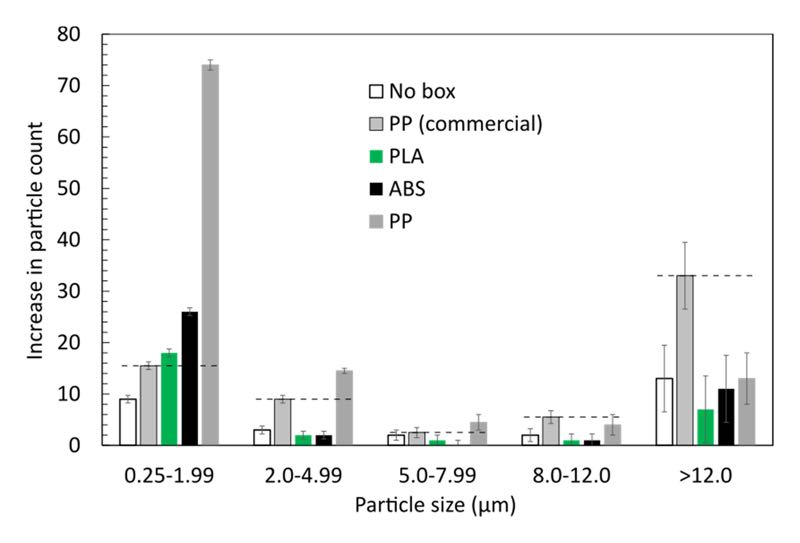
Figure 2. Increase in particle count during 15 days storage in various single wafer boxes. The initial number of particles on all wafers were in the order of 10-20. The dashed lines indicate reference levels set by the commercial PP box, which is commonly used in cleanrooms. The error bars are determined from the variation in several repeated measurements
The dynamic test also found promising results. It showed that normal operation of the 3D-printed positioner would cause a limited increase in the number of particles on the measured wafer. There seems to be a higher increase near mechanical parts due to abrasion, which may, however, be insignificant for applications that do not require to maintain a remarkably high level of cleanliness in the environment (as opposed to photolithography and high-temperature anneal areas, for instance).
Finally, the particles generated are not overly harmful. The commercial and 3D-printed PP, both of which contain no intentionally-added colourants, show similar metal contents. More accurately, Al concentration in the commercial box substance is slightly higher than that of the 3D-printed equivalent, which indicates that the 3D-printed PP box is at least equally cleanroom compatible as the commercially available products from a contamination perspective.
Comparison with the wafer boxes indicated that, for normal operation of the positioner (wafer placed inside the clamp), particle generation was in the same range as in commercial and 3D-printed wafer boxes. More particles are generated near the mechanical parts and can diffuse in the environment, thus regular cleaning of those part is recommended.
Care must be taken, however, in the selection of the 3D printing materials. Those with colourants or unknown chemical ingredients are not recommended without further testing.
The bottom line is that 3D-printed components and tools, such as wafer boxes, tweezers, wafer holders or wafer positioners, fulfil the strict particle generation and chemical compatibility requirements set for items used in cleanrooms and can be 3D-printed from readily-available low-cost thermopolymers.
References
Full details of the first study can be found at: Ismo T. S. Heikkinen, Christoffer Kauppinen, Zhengjun Liu, Sanja M. Asikainen, Steven Spoljaric, Jukka V. Seppälä, Hele Savin, and Joshua M. Pearce. Chemical Compatibility of Fused Filament Fabrication-based 3-D Printed Components with Solutions Commonly Used in Semiconductor Wet Processing. Additive Manufacturing 23, pp. 99-107 (2018). Digital Open Access.
Full details of the second study can be found at: T.P.Pasanen, G.von Gastrow, I.T.S.Heikkinen, V.Vähänissi, H.Savin, J.M.Pearce. Compatibility of 3-D printed devices in cleanroom environments for semiconductor processing. Materials Science in Semiconductor Processing 89 (2019), pp. 59-67. Digital Open Access.


