The first semiconductor revolution was built around the silicon microprocessor. Then the first Intel microprocessors appeared in the early 1970s, with typically 2,300 transistors per chip. Improvements in processing technology allowed engineers to shrink transistor size so that more transistors could be crammed onto a chip—a trend that became known as Moore's Law, following observations by Gordon Moore, CEO of Intel.
Transistor count translates into computing power, with more powerful microprocessors handling larger amounts of data. In his 1999 book Business at the speed of thought, Bill Gates predicted the digitisation of data, from maps to music, photographs and videos, enabling transmission over communication networks. At the time, his vision appeared futuristic, but technological advances have more than kept pace.
Throughout the silicon revolution, the cost of silicon chips has not significantly changed; the microprocessor in a modern smartphone has around four billion transistors, and costs typically US$60. However, the cost of infrastructure required to build these chips has increased dramatically.
It now costs between $3bn-4bn to build a silicon chip fabrication plant (fab plant), and consequently, there are relatively few fabs around the world.
Andy Sellars, CSA Catapult
This trend in fabrication costs has seen silicon chip fabrication migrate to fabs in the far east. China recently announced a $24bn giga-fab—a facility with a monthly production capacity of 100,000 wafers or more—as part of a strategy to become self-sufficient in silicon chip manufacture.
As it turns out, it's no longer cost-effective to manufacture silicon chips in the UK, and UK fabrication has steadily been offshored.
Although the UK no longer manufactures silicon chips, Britain has emerged as a world leader in "fabless design". Companies such as Cambridge-based ARM design the microprocessor architecture while fabs in the far east manufacture the chips. Arguably, the UK captures much of the value of design through licensing, but all the manufacturing value is captured overseas.
Next-generation semiconductors
Silicon chip performance has improved dramatically over the years, but recent societal trends and new emerging technologies demand further improvements that cannot be delivered using silicon alone.
Next generation chips will use compound semiconductors (CS) that combine two or more elements from the periodic table to create a compound. Examples include gallium nitride (GaN) and indium phosphide (InP).
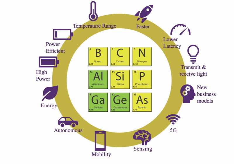
Table of elements illustrates next-gen electronics powered by compound semiconductors
CSs have properties that outperform silicon in three application areas:
- Speed: compound semiconductors can operate at much higher frequencies compared to silicon, which is required for high-speed data transfer over 5G networks
- Light: compound semiconductors emit and detect light efficiently, making them suitable for 3D sensors in health diagnostics or facial recognition. While silicon can detect light, it has limited detection efficiency, and it cannot emit light
- Power: compound semiconductors can handle much higher power levels than silicon with lower losses, which mean they will extend the range of electric vehicles
These attributes translate into healthy growth forecasts for the CS industry, and though CSs will not replace silicon; they will complement its computing power.
The global silicon market is worth around $300bn, while the CS market is worth $74bn. Interestingly though, the silicon market is growing at 2-3% CAGR, while the CS market enjoys growth rates of typically 12-15% CAGR, depending on the application.
The UK has around 10% of this global CS market, equating to about $7.4bn. At current growth rates, the CS market is forecast to be worth $308bn by 2030—and the UK has the potential to take an increasing share of this growing market.
If compound semiconductors are so good, why are they not used more widely? The fact is that CSs have been around since the 1950s, but they have never seen the high-volume applications of silicon. This low utilisation rate is due to their performance and cost characteristics, which are best illustrated regarding the supply chain on the infographic below.
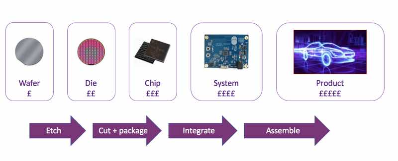
Supply chain: the low utilisation rate of compound semiconductors is due to their performance and cost ratio
The supply chain typically consists of five stages: from wafer to die, then chip, system and product. The CS supply chain is similar to the silicon supply chain: transistors are etched into the wafer using a process called lithography to create an array of chips on a die. The chips are then cut from the die, individually packaged before being integrated into systems, and finally assembled into products. Typically, the value increases by 5x or 10x from one stage to another.
Wafer production process
In the case of silicon, the wafer is a single crystalline material that can be grown with very high levels of purity. This makes it ideal for high volume scale-up with modern silicon chips created from 450mm-diameter silicon wafers.
This scalability has maintained the high performance/cost ratio for silicon chips; it has also fuelled the large capital investments required for fab infrastructure.
In the case of CS, the wafer is created using a process known as epitaxial growth: atoms are deposited one layer at a time under vacuum conditions within a cleanroom. This process is highly complex and harder to scale. The largest wafers are 150 mm in diameter, but more typically 100 mm.
CS die is often harder to handle than silicon dies, and they require special packaging processes. To exploit the performance and cost benefits of CS it is often necessary to design a system from the ground up, paying particular attention to the silicon-CS interface. This creates challenges for industrial scale-up, which require R&D investment to overcome.
Fortunately, the UK is in a leading position having invested over £750m in research and innovation over the past decade, supported by The Engineering and Physical Sciences Research Council (EPSRC) and Innovate UK, both part of the United Kingdom Research and Innovation (UKRI).
Bridging the gap
The compound semiconductor cluster in South Wales has received considerable public and private sector investments. This cluster is a collection of interrelated businesses and research organisations that operate under the brand CS-Connected.
The Catapult is a £50m initiative to help UK companies develop new products and services that exploit the superior performance of compound semiconductors, accelerating their adoption into mainstream applications
The cluster covers pure research-to-applications and spans the breadth of the supply chain. With recent equipment investments exceeding £300m, it is globally unique for enabling companies to rapidly iterate from design to prototype and to production within a small geographical region.
The Compound Semiconductor Applications Catapult (CSA Catapult) plays a pivotal role in the CS-Connected cluster. The Catapult is a £50m investment established by Innovate UK, which operates as a non-profit research and technology organisation (RTO).
The role of the Catapult is to help UK companies develop new products and services that exploit the superior performance of compound semiconductors, accelerating their adoption into mainstream applications, which will drive economic and social benefits to the UK.
The Catapult's innovation centre focuses on three applications areas:
- Speed (RF and microwave technologies)
- Light (photonics and sensors)
- Power (power electronics)
The Catapult has a suite of simulation and modelling tools and an advanced packaging laboratory to overcome the innovation challenges described above. It also has a market intelligence unit that monitors trends and drivers, helping to inform industry leaders.
Future trends
Emerging technologies, such as artificial intelligence (AI) and quantum computing, require compound semiconductors to achieve full commercialisation. The UK has a rich heritage of microprocessor design, with companies such as ARM and Imagination Technologies, and a new breed of start-up companies designing AI processors, such as Bristol-based GraphCore. AI processors need sensors to map their environment—and this is where compound semiconductors can provide 3D visualisation.
Similarly, quantum computing and quantum cryptography require precise lasers to "freeze" atoms so they operate close to absolute zero. Such an operation will be achieved with compound semiconductor lasers, ultimately creating a quantum system on a chip—something that might be some years away.
The CSA Catapult is closely monitoring these technologies, looking to help companies commercialise their designs sooner.
While compound semiconductors have been around for some time, many barriers have held back their true potential. That is about to change.
What's on at CSA Catapult
There are over 5,000 companies that manufacture electronic systems in the UK, and many of these companies develop products that could use compound semiconductors in the future. The Catapult is currently working with companies developing electric vehicle propulsion systems and novel imaging technologies.
The Catapult can provide bespoke research on a one-to-one basis, or work as part of a supply chain consortium, accessing funds for research and development. The team is highly experienced at navigating the funding landscape, helping companies access R&D grants to overcome their innovation challenges.
The UK's funding landscape has undergone a major overhaul recently with the launch of the Industrial Strategy in November 2017, which aims to raise R&D investment to 2.4% of GDP. This ambitious target equates to £4.7bn in just four years, with the aim to raise productivity while delivering social benefits across the UK.
N.B. This article is featured in the July 2019 issue of Cleanroom Technology. The latest digital edition is available online.