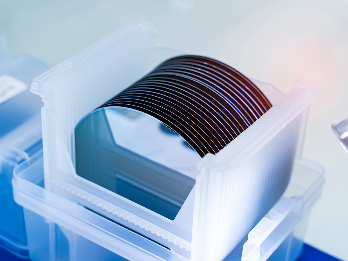
Cleanrooms run on control. Anything introduced must neither shed particles nor release molecules or ions that raise background levels above class limits. For wafers, the main risks typically include trace metals and particles, followed by organic residues that may remain on the wafer surface.
When startups and scaleups collaborate with research centres for semiconductor component processing in the latter’s cleanroom, there may be concern over whether wafers are clean enough not to compromise the space for all users. In such situations, the best practice is to analyse the wafers for trace contaminant presence before bringing them into the facility.
To ensure that relevant contaminants are detected with sufficiently low detection limits, state-of-the-art techniques specifically developed for wafer analysis are required. This article summarises the key methods employed with practical examples of analysis workflows where several methods are used to confirm cleanroom compatibility.
Factors to consider during method selection
The primary factor in choosing a cleanroom compatibility test is the type of contamination being evaluated. Once suitable techniques for that contaminant type are identified, secondary considerations such as detection limits, sample compatibility (wafer size, substrate, and any coating or thin film), turnaround time, and cost become important for optimising the analysis plan.
The list below summarises how these factors influence the choice of analytical methods under different practical constraints:
- Target contaminants: For particle contamination on silicon and other wafers, optical particle counting is the go-to method, with possible follow-up analysis with SEM-EDX to identify detected particles. VPD-ICP-MS and TXRF are the top choices for trace metal analysis, and ATD-GC-MS for detecting volatile and semi-volatile organic residues.
- Detection limits: Since the smallest amounts of contaminants can compromise cleanroom integrity, detection limits must be exceptionally low. VPD-ICP-MS is one of the most sensitive trace metal analysis methods available, with detection limits in the range of 10⁶–10¹⁰ at/cm² depending on the element. Particle counters vary in sensitivity, so instrument selection must match the required size threshold.
- Analysis target area: Some techniques, such as VPD-ICP-MS, analyse the full wafer surface (with possible edge exclusion), while others, such as TXRF, can map the surface to localise where contaminants are concentrated.
- Turnaround and pricing: A high-throughput, relatively cost-effective method such as VPD-ICP-MS is recommended for routine analysis and projects with tight deadlines. In-depth investigations into the origins of contamination may require analysis techniques with longer processing times and higher pricing.
The following sections go into further detail about the applications of our recommended methods for wafer cleanroom suitability analysis.
The primary factor in choosing a cleanroom compatibility test is the type of contamination being evaluated
Particle counting for fast assessment of particulate contamination levels
As cleanroom classifications defined in the ISO 14644 standard series are based on allowable particle concentrations, optical particle counting is often the first step in verifying the cleanroom suitability of wafers. The instrument should be selected according to


