

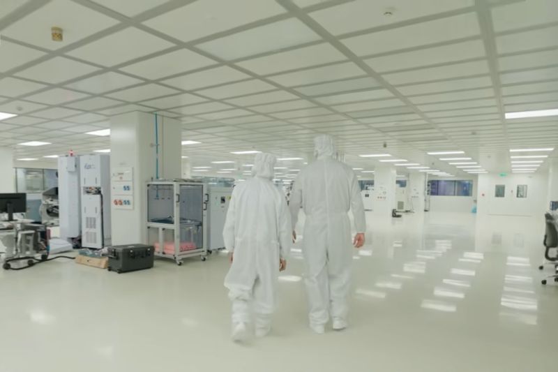
HCLTech has opened a new 40,000 sqft Advanced Semiconductor Lab in Bengaluru, India, including 25,000 sqft of ISO Class 6 and 7 cleanroom space.
The global technology and engineering services company said the laboratory will serve both domestic and international semiconductor markets.
The facility was opened on 8 September and has been developed to support semiconductor post-silicon engineering, advanced testing and failure analysis, with the cleanroom housing automated test equipment, probes, qualification chambers and failure analysis systems.
Equipment at the facility includes systems from Teradyne, Advantest, Keysight, Tektronix and Thermo Fisher Scientific.
The laboratory has been established with an investment of Rs 185 crore ($19.3m) and is intended to support research and development, pre-production and production qualification for semiconductor components.
The cleanroom also includes optical and electron microscopy equipment and focused ion beam systems for semiconductor failure analysis.
HCLTech said the laboratory will provide electrical validation, automated testing, qualification and failure analysis within a single facility, supporting the development process from design specifications through to finished semiconductor parts.
The company said the facility is also set to achieve certifications including ISO 17025, ISO 9001, AS 9100 for the military and aerospace sector, and ISO 13485 for medical devices.


