

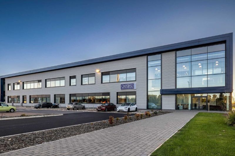
Oxford Instruments Plasma Technology has opened a 1,200 sqm cleanroom facility in Bristol, expanding its capacity for demonstrating semiconductor processing technologies.
The facility houses 35 systems and provides a controlled environment for evaluating plasma processing equipment and applications, including etching, deposition, atomic layer deposition (ALD) and atomic layer etch (ALE).
The facility was designed and delivered by architecture practice Corstorphine & Wright, which was appointed by Hillwood and Oxford Instruments for the project.
Construction began in May 2021, with the development incorporating offices, production space and ISO Class 5 and 6 application research laboratories.
The ISO Class 5 and 6 cleanroom is designed to replicate the quality and stability of production environments, enabling customers to assess process performance and repeatability using wafers up to 200 mm in diameter.
The expanded facility provides 50% more demonstration systems, supporting applications ranging from research and development to high-volume semiconductor manufacturing.
Plasma processing and contamination control
The cleanroom accommodates a range of plasma processing technologies used in semiconductor manufacturing and advanced materials research.
Available systems include inductively coupled plasma (ICP) and reactive ion etching (RIE), ion beam etching and deposition, chemical vapour deposition (CVD), plasma-enhanced chemical vapour deposition (PECVD), and ALD equipment for research and production applications.
The systems support work across compound semiconductors, power electronics, optoelectronics, microLEDs and other emerging technologies.
Equipment health checks and routine maintenance are carried out using the company's PTIO user interface, with procedures intended to maintain consistent operating conditions and minimise downtime.
The facility also uses statistical analysis and experimental design tools, including JMP software, to assess process trends, repeatability and performance. These capabilities allow demonstrations to be tailored to individual customer applications.
Expanded metrology capabilities
The Bristol facility also incorporates metrology equipment for inspecting and characterising semiconductor structures and customer samples.
Two high-resolution scanning electron microscopy (SEM) systems have been installed, expanding the facility's capabilities in imaging and materials analysis.
Other equipment supports focused ion beam (FIB) milling, atomic force microscopy (AFM), Raman microscopy and thin-film characterisation.
The metrology laboratory incorporates vibration-control measures to support sensitive measurements.
Equipment is installed on a thick concrete base, while selected instruments are mounted on vibration-isolation platforms with active vibration cancellation.
Combining plasma processing with metrology allows customers to examine fabricated structures and assess their material properties as part of the same demonstration process.


