
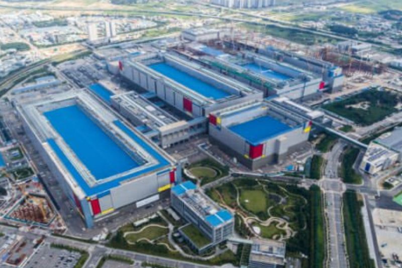
Samsung Electronics has accelerated the cleanroom construction schedule at its Pyeongtaek Fab 5 (P5) facility in South Korea.
The company has advanced core infrastructure work by several months as part of its broader “Shell First” strategy of securing production space ahead of market demand.
Originally planned to begin full-scale cleanroom construction in early 2027, the company now has preliminary insert work scheduled for Q4 this year.
Following a request to construction partners, preparatory works have been rescheduled to Q2 and cleanroom build-out is now expected to begin in early Q3.
Piping installation, crucial to enabling semiconductor equipment deployment, has also been brought forward to the end of this year.
Cleanrooms offer environmentally controlled spaces to regulate particulate levels, temperature, humidity, and pressure to meet the exacting requirements of chip fabrication.
The company has said that cleanrooms must be completed before any semiconductor manufacturing tools can be installed, making this a critical inflection point in fab build-outs.
What is the Shell First strategy?
Samsung’s Shell First strategy involves completing fab infrastructure such as cleanrooms ahead of committing to full equipment capital expenditure, allowing the company to respond quickly to shifts in demand.
During its recent earnings call, Samsung reiterated its intention to maintain pre-emptive investment in fab capacity, with rapid equipment deployment following when market trends justify it.
The acceleration of P5’s cleanroom works comes as Samsung has also reported strengthened competitive momentum in memory markets.
Recent figures indicate the company reclaimed its position as the largest global DRAM supplier in Q4, driven in part by HBM sales growth.
How the P5 fab is part of the larger Samsung portfolio
The P5 facility is designed to be larger than existing fabs at Samsung’s Pyeongtaek campus, with six cleanrooms spread across three floors versus four cleanrooms across two floors at earlier plants.
Samsung has described P5 as a future hub for HBM production, positioning it to support demand expected from AI and data-centre markets.
The total investment across Samsung Electronics’ Pyeongtaek semiconductor campus is estimated to span tens of billions of dollars, with individual fabs like P5 projected at $23–46 bn.
Industry data shows that memory demand, especially for HBM used in AI accelerators and high-performance computing, has surged, prompting both Samsung and rivals to bring forward cleanroom schedules and early production targets.
In a previous cleanroom‑related milestone, Samsung Electronics broke ground on a new EUV semiconductor line at its Hwaseong campus in Korea back in 2018.
The US $6 bn facility is aimed at advanced process technology under 7 nm that helped anchor the company’s semiconductor cluster spanning Giheung, Hwaseong, and Pyeongtaek.


